Microchip PIC24FJ256GA108-I/PT: A Comprehensive Technical Overview
The Microchip PIC24FJ256GA108-I/PT stands as a prominent member of the PIC24F family, representing a robust 16-bit architecture engineered for a wide spectrum of embedded applications. This microcontroller unit (MCU) is particularly suited for demanding tasks in the industrial, medical, and consumer electronics sectors, where a blend of processing power, peripheral integration, and power efficiency is paramount.
At the heart of this device lies a high-performance 16-bit modified Harvard architecture CPU core. Operating at a maximum frequency of 16 MIPS (Million Instructions Per Second), it delivers a significant performance boost over traditional 8-bit MCUs while maintaining a favorable power profile. The core is augmented with a 17-bit by 17-bit single-cycle hardware multiplier and a 32-bit by 16-bit hardware divider, accelerating computational tasks and making it an excellent choice for digital signal processing (DSP) and control algorithms.
A defining feature of this MCU is its substantial 256 KB of self-programmable Flash memory. This non-volatile memory provides ample space for complex application code and offers the flexibility for field firmware updates. Complementing this is 16 KB of RAM, ensuring smooth operation for data-intensive applications and real-time operating systems (RTOS).
The peripheral set integrated into the PIC24FJ256GA108-I/PT is both extensive and versatile, designed to minimize external component count and simplify system design. Key peripherals include:
Five 16-bit Timers/Counters: Offering exceptional flexibility for waveform generation, event timing, and capture/compare operations.
Dual Direct Memory Access (DMA) Controllers: These controllers allow data to be transferred between peripherals and memory without CPU intervention, drastically improving system efficiency and reducing power consumption by allowing the core to remain in idle mode.

Real-Time Clock and Calendar (RTCC): A crucial feature for time-keeping applications, operating from a low-power 32.768 kHz oscillator.
Hardware Crypto Engine: Accelerates AES and DES/SHA algorithms, providing a critical layer of security for connected devices.
Communication Interfaces: The device is equipped with a comprehensive suite of serial communication modules, including multiple UART, SPI, and I²C™ modules, facilitating easy connection to a vast array of sensors, displays, and other peripherals.
The "GA" in its part number signifies its integrated hardware graphics controller. This dedicated peripheral can drive graphical displays directly, offloading the CPU from the intensive task of managing the display buffer, making it ideal for human-machine interface (HMI) applications.
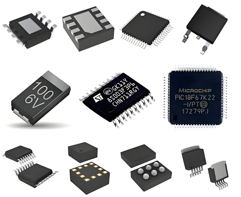
Housed in a 100-pin TQFP package, the MCU offers a high number of general-purpose I/O pins, providing ample connectivity for complex projects. Its industrial temperature rating (-40°C to +85°C) ensures reliable operation in harsh environments.
In summary, the PIC24FJ256GA108-I/PT is a feature-rich, high-performance 16-bit microcontroller. Its combination of processing muscle, large memory, advanced security, and a diverse set of integrated peripherals—most notably the integrated hardware graphics controller and DMA controllers—makes it a powerful and efficient solution for next-generation embedded designs.
ICGOOODFIND: The PIC24FJ256GA108-I/PT is a top-tier choice for developers seeking a 16-bit MCU that balances performance with low-power operation. Its standout features, including the graphics controller, crypto engine, and DMA, make it exceptionally well-suited for advanced HMI, industrial control, and secure IoT applications.
Keywords: 16-bit MCU, Hardware Graphics Controller, DMA Controllers, AES Crypto Engine, Low-Power Operation.
